Präsentation herunterladen
Die Präsentation wird geladen. Bitte warten

1
Embedded System Hardware - Processing -
Peter Marwedel Informatik 12 TU Dortmund Germany © Springer, 2010 2012年 11 月 20 日 These slides use Microsoft clip arts. Microsoft copyright restrictions apply.

2
Efficiency: slide from lecture 1 applied to processing
CPS & ES must be efficient Code-size efficient (especially for systems on a chip) Run-time efficient Weight efficient Cost efficient Energy efficient © Graphics: Microsoft, P. Marwedel, M. Engel, 2011
 Run-time efficient. Weight efficient. Cost efficient. Energy efficient. © Graphics: Microsoft, P. Marwedel, M. Engel,")
3
Key idea of very long instruction word (VLIW) computers (1)
Instructions included in long instruction packets. Instruction packets are assumed to be executed in parallel. Fixed association of packet bits with functional units. Compiler is assumed to generate these “parallel” packets

4
Key idea of very long instruction word (VLIW) computers (2)
Complexity of finding parallelism is moved from the hardware (RISC/CISC processors) to the compiler; Ideally, this avoids the overhead (silicon, energy, ..) of identifying parallelism at run-time. A lot of expectations into VLIW machines However, possibly low code efficiency, due to many NOPs Explicitly parallel instruction set computers (EPICs) are an extension of VLIW architectures: parallelism detected by compiler, but no need to encode parallelism in 1 word.
 to the compiler; Ideally, this avoids the overhead (silicon, energy, ..) of identifying parallelism at run-time. A lot of expectations into VLIW machines. However, possibly low code efficiency, due to many NOPs. Explicitly parallel instruction set computers (EPICs) are an extension of VLIW architectures: parallelism detected by compiler, but no need to encode parallelism in 1 word.")
5
EPIC: TMS 320C6xxx as an example
1 Bit per instruction encodes end of parallel exec. 1 1 1 1 Instr. A Instr. B Instr. C Instr. D Instr. E Instr. F Instr. G Cycle Instruction 1 A 2 B C D 3 E F G Instructions B, C and D use disjoint functional units, cross paths and other data path resources. The same is also true for E, F and G.

6
Partitioned register files
Many memory ports are required to supply enough operands per cycle. Memories with many ports are expensive. Registers are partitioned into (typically 2) sets, e.g. for TI C6xxx: Parallel execution cannot span several packets IA64
 sets, e.g. for TI C6xxx: Parallel execution cannot span several packets IA64.")
7
More encoding flexibility with IA-64 Itanium
3 instructions per bundle: instruc instruc instruc template 127 There are 5 instruction types: A: common ALU instructions I: more special integer instructions (e.g. shifts) M: Memory instructions F: floating point instructions B: branches The following combinations can be encoded in templates: MII, MMI, MFI, MIB, MMB, MFB, MMF, MBB, BBB, MLX with LX = move 64-bit immediate encoded in 2 slots Instruction grouping information
 M: Memory instructions. F: floating point instructions. B: branches. The following combinations can be encoded in templates: MII, MMI, MFI, MIB, MMB, MFB, MMF, MBB, BBB, MLX with LX = move 64-bit immediate encoded in 2 slots. Instruction grouping information.")
8
Templates and instruction types
End of parallel execution called stops. Stops are denoted by underscores. Example: bundle 1 bundle 2 … MMI M_II MFI_ MII MMI MIB_ Group 1 Group 2 Group 3 Very restricted placement of stops within bundle. Parallel execution within groups possible. Parallel execution can span several bundles

9
Itanium® 9300 (Tukwila), 2010 2 G transistors 4 cores
8-fold hyper-threading/core 1.5 GHz at 1.3V [ pressroom/emea/deu/ htm] © Intel, 2010

10
Large # of delay slots, a problem of VLIW processors
add sub and or sub mult xor div ld st mv beq

11
Large # of delay slots, a problem of VLIW processors
add sub and or sub mult xor div ld st mv beq

12
Large # of delay slots, a problem of VLIW processors
The execution of many instructions has been started before it is realized that a branch was required. add sub and or sub mult xor div ld st mv beq Nullifying those instructions would waste compute power Executing those instructions is declared a feature, not a bug. How to fill all “delay slots“ with useful instructions? Avoid branches wherever possible.

13
Predicated execution: Implementing IF-statements “branch-free“
Conditional Instruction “[c] I“ consists of: condition c (some expression involving condition code regs) instruction I c = true I executed c = false NOP
 instruction I. c = true I executed. c = false NOP.")
14
Predicated execution: Implementing IF-statements “branch-free“: TI C6xxx
Conditional branch [c] B L1 NOP 5 B L2 NOP 4 SUB x,y,a || SUB x,z,b L1: ADD x,y,a || ADD x,z,b L2: Predicated execution [c] ADD x,y,a || [c] ADD x,z,b || [!c] SUB x,y,a || [!c] SUB x,z,b if (c) { a = x + y; b = x + z; } else { a = x - y; b = x - z; max. 12 cycles 1 cycle
 { a = x + y; b = x + z; } else. { a = x - y; b = x - z; max. 12 cycles. 1 cycle.")
15
Energy efficiency reached with VLIW processors
“inherent power efficiency of silicon“ © Hugo De Man: From the Heaven of Software to the Hell of Nanoscale Physics: An Industry in Transition, Keynote Slides, ACACES, 2007 © Silicon Hive 41 Issue VLIW for SDR 130 nm, 1,2 V, 6,5mm², 16 bit 30 operations/cycle (OFDM) 150 MHz, 190 mW (incl. SRAMs) 24 GOPs/W, ~1/5 IPE
 150 MHz, 190 mW (incl. SRAMs) 24 GOPs/W, ~1/5 IPE.")
16
Microcontrollers - MHS 80C51 as an example -
8-bit CPU optimised for control applications Extensive Boolean processing capabilities 64 k Program Memory address space 64 k Data Memory address space 4 k bytes of on chip Program Memory 128 bytes of on chip data RAM 32 bi-directional and individually addressable I/O lines Two 16-bit timers/counters Full duplex UART 6 sources/5-vector interrupt structure with 2 priority levels On chip clock oscillators Very popular CPU with many different variations Features 4 Embedded Systems

17
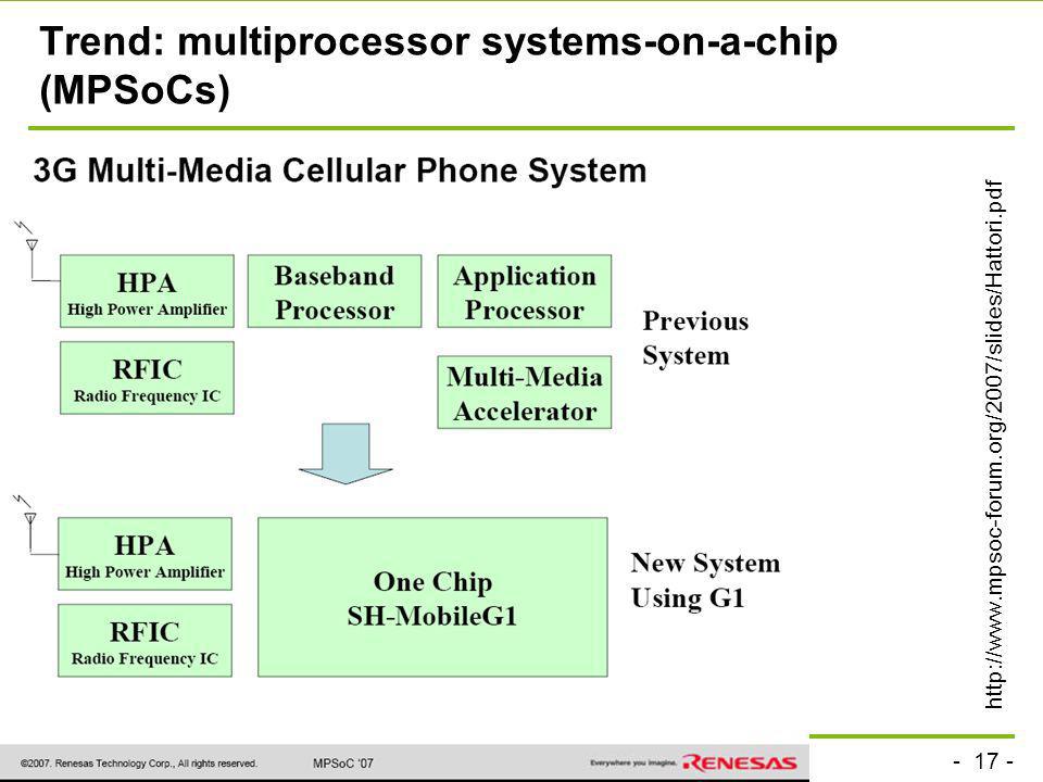
Trend: multiprocessor systems-on-a-chip (MPSoCs)
18
Embedded System Hardware - Reconfigurable Hardware -
Peter Marwedel Informatik 12 TU Dortmund Germany © Springer, 2010 2012年 11 月 20 日 These slides use Microsoft clip arts. Microsoft copyright restrictions apply.

19
Energy Efficiency of FPGAs
“inherent power efficiency of silicon“ © Hugo De Man, IMEC, Philips, 2007

20
Reconfigurable Logic Custom HW may be too expensive, SW too slow.
Combine the speed of HW with the flexibility of SW HW with programmable functions and interconnect. Use of configurable hardware; common form: field programmable gate arrays (FPGAs) Applications: algorithms like de/encryption, pattern matching in bioinformatics, high speed event filtering (high energy physics), high speed special purpose hardware. Very popular devices from XILINX, Actel, Altera and others
 Applications: algorithms like de/encryption, pattern matching in bioinformatics, high speed event filtering (high energy physics), high speed special purpose hardware. Very popular devices from. XILINX, Actel, Altera and others.")
21
Floor-plan of VIRTEX II FPGAs

22
Interconnect for Virtex II
Hierarchical Routing Resources; More recent: Virtex 5, 6, 7 no routing plan found for Virtex 7.

23
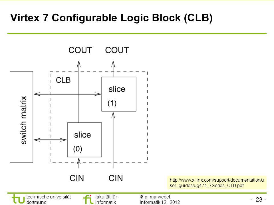
Virtex 7 Configurable Logic Block (CLB)
24
Virtex 7 Slice (simplified)
Memories typically used as look-up tables to implement any Boolean function of 6 variables. Processors typically implemented as “soft cores” (microblaze)
")
25
Virtex 7 SliceM SliceM supports using memories for storing data and as shift registers © Xilinx

26
Resources available in Virtex 7 devices (max)
XC7V2000T Logic cells 1,954,560 Slices 305,400 Max distributed RAM [Kb] 21,550 DSP slices 2,160 Block RAM blocks 18 Kb 2,584 Block RAM blocks 36 Kb 1,292 Block RAM blocks Max [Kb] 46,512 PCIe 4 GTX Transceivers 36 A/D converters 1 User I/O 1,200 [

27
Virtex-7 FPGAs Maximum Capability Virtex-7 T Virtex-7 XT Virtex-7 HT
Logic density 1,995 k 1,139 k 864 k Peak transceiver speed 12.5 Gb/s (GTX) 13.1 Gb/s (GTH) 28.05 Gb/s (GTZ) Peak bi-directional bandwidth 0.9 Tb/s 2.515 Tb/s 2.784 Tb/s DSP throughput (symmetric filter) 2,756 G MACS 5,314 GMACS 5,053 GMACS Block RAM 46.5 Mb 85 Mb 64.4 Mb I/O pins 1,200 1,100 700
 13.1 Gb/s (GTH) Gb/s (GTZ) Peak bi-directional bandwidth. 0.9 Tb/s Tb/s Tb/s. DSP throughput (symmetric filter) 2,756 G MACS. 5,314 GMACS. 5,053 GMACS. Block RAM Mb. 85 Mb Mb. I/O pins. 1,200. 1,")
28
Memory © Springer, 2010 2012年 11 月 20 日 These slides use Microsoft clip arts. Microsoft copyright restrictions apply.

29
Memory Oops! Memories! For the memory, efficiency is again a concern:
capacity energy efficiency speed (latency and throughput); predictable timing size cost other attributes (volatile vs. persistent, etc)
; predictable timing. size. cost. other attributes (volatile vs. persistent, etc)")
30
Memory capacities expected to keep increasing
[ITRS Update 2008]

31
Where is the power consumed? - Stationary systems -
According to International Technology Roadmap for Semi-conductors (ITRS), 2010 update, [ © ITRS, 2010 Switching power, logic dominating Overall power consumption a nightmare for environmentalists
, 2010 update, [ © ITRS, Switching power, logic dominating. Overall power consumption a nightmare for environmentalists.")
32
Where is the power consumed? - Consumer portable systems -
According to International Technology Roadmap for Semi-conductors (ITRS), 2010 update, [ Based on current trends © ITRS, 2010 Memory and logic, static and dynamic relevant Following current trends will violate maximum power constraint (0.5-1 W).
, 2010 update, [ Based on current trends. © ITRS, Memory and logic, static and dynamic relevant. Following current trends will violate maximum power constraint (0.5-1 W).")
33
Memory energy significant even if we take display and RF of mobile device into account
[O. Vargas (Infineon Technologies): Minimum power consumption in mobile-phone memory subsystems; Pennwell Portable Design - September 2005;] Thanks to Thorsten Koch (Nokia/ Univ. Dortmund) for providing this source. 33
: Minimum power consumption in mobile-phone memory subsystems; Pennwell Portable Design - September 2005;] Thanks to Thorsten Koch (Nokia/ Univ. Dortmund) for providing this source. 33.")
34
Energy consumption and access times of memories
Example CACTI: Scratchpad (SRAM) vs. DRAM (DDR2): DRAM SRAM 16 bit read; size in bytes; 65 nm for SRAM, 80 nm for DRAM Source: Olivera Jovanovic, TU Dortmund, 2011
 vs. DRAM (DDR2): DRAM. SRAM. 16 bit read; size in bytes; 65 nm for SRAM, 80 nm for DRAM. Source: Olivera Jovanovic, TU Dortmund,")
35
Access times and energy consumption for multi-ported register files
Cycle Time (ns) Area (l2x106) Power (W) We have used the Rixner model to evaluate cycle time, area and power for these register files. These graphs show the figures for the 0.18 mm technology as the register file size is increased. Blue lines are for 2 memory ports, the others are for 3 memory poerts. On a VLIW processor, the cycle time can be bounded by the register file, since in these processors the register file is the main central structure. From now on, we will assume that the access time to register file determines the processor cycle time. Source and © H. Valero, 2001 Rixner’s et al. model [HPCA’00], Technology of 0.18 mm
 Area (l2x106) Power (W) We have used the Rixner model to evaluate cycle time, area and power for these register files. These graphs show the figures for the 0.18 mm technology as the register file size is increased. Blue lines are for 2 memory ports, the others are for 3 memory poerts. On a VLIW processor, the cycle time can be bounded by the register file, since in these processors the register file is the main central structure. From now on, we will assume that the access time to register file determines the processor cycle time. Source and © H. Valero, Rixner’s et al. model [HPCA’00], Technology of 0.18 mm.")
36
Trends for the Speeds Speed gap between processor and main DRAM increases Similar problems also for embedded systems & MPSoCs Memory access times >> processor cycle times “Memory wall” problem 8 Speed CPU Performance (1.5-2 p.a.) 4 2x every 2 years 2 DRAM (1.07 p.a.) 1 years 1 2 3 4 5 [P. Machanik: Approaches to Addressing the Memory Wall, TR Nov. 2002, U. Brisbane] 36
 4. 2x every 2 years. 2. DRAM (1.07 p.a.) 1. years [P. Machanik: Approaches to Addressing the Memory Wall, TR Nov. 2002, U. Brisbane] 36.")
37
However, clock speed increases have come to a halt
Copyright © 2011, Elsevier Inc. All rights Reserved. [Hennessy/Patterson: Computer Architecture, 5th ed., 2011] The speed gap does not disappear – may be, it is not getting larger any more.

38
Set-associative cache n-way cache
Address Tag Index $ (€) way 0 way 1 Tags data block Tags data block = = 1 Data
 way 0. way 1. Tags. data block. Tags. data block. = = 1. Data.")
39
Hierarchical memories using scratch pad memories (SPM)
SPM is a small, physically separate memory mapped into the address space Address space Examples: Most ARM cores allow tightly coupled memories IBM Cell Infineon TriCore Many multi-cores, due to high costs of coherent caches scratch pad memory FFF.. Hierarchy no tag memory main SPM processor SPM select Selection is by an appropriate address decoder (simple!)
")
40
Comparison of currents using measurements
E.g.: ATMEL board with ARM7TDMI and ext. SRAM /3

41
Why not just use a cache ? Energy for parallel access of sets, in comparators, muxes. [R. Banakar, S. Steinke, B.-S. Lee, 2001]

42
Influence of the associativity
Parameters different from previous slides [P. Marwedel et al., ASPDAC, 2004]

43
Summary Processing VLIW/EPIC processors MPSoCs FPGAs Memories
“Small is beautiful” (in terms of energy consumption, access times, size)
")
44
SPARE SLIDES

45
Instruction types are mapped to functional unit types
There are 4 functional unit (FU) types: M: Memory Unit I: Integer Unit F: Floating-Point Unit B: Branch Unit Instruction types corresponding FU type, except type A (mapping to either I or M-functional units).
 types: M: Memory Unit. I: Integer Unit. F: Floating-Point Unit. B: Branch Unit. Instruction types corresponding FU type, except type A (mapping to either I or M-functional units).")
46
Nevertheless, (parallel) performance keeps increasing
Copyright © 2011, Elsevier Inc. All rights Reserved. [Hennessy/Patterson: Computer Architecture, 5th ed., 2011]

47
Philips TriMedia- Processor
For multimedia-applications, up to 5 instruc-tions/cycle. PNX15XX_SER_N_3.pdf (incompatible with firefox?) © NXP
 © NXP.")
48
Similar information according to other sources
IEEE Journal of SSC Nov. 96 [Based on slide by and ©: Osman S. Unsal, Israel Koren, C. Mani Krishna, Csaba Andras Moritz, U. of Massachusetts, Amherst, 2001] [Segars 01 according to 48

49
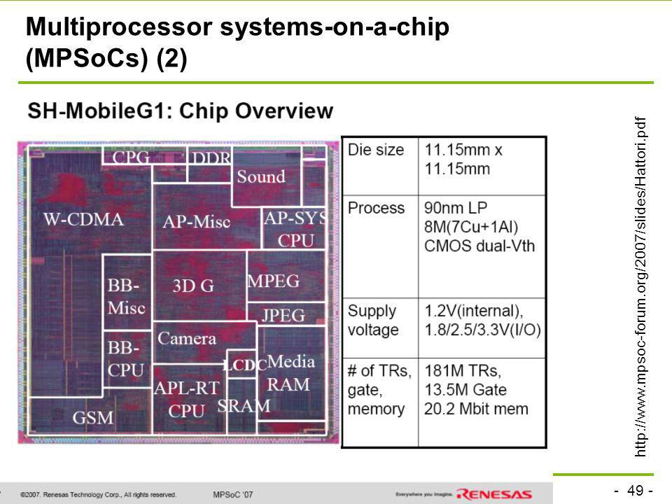
Multiprocessor systems-on-a-chip (MPSoCs) (2)
50
TriMedia- Processor Lastest version: starting 5-8 operations per cycle
© Trident, 2010 (since 2012/1 under chapter 11)
")
Ähnliche Präsentationen


