Präsentation herunterladen
Die Präsentation wird geladen. Bitte warten

1
Problems, Solutions, Limitations
Transient and Permanent Faults in Nanoelectronic ICs: Compensation and Repair Problems, Solutions, Limitations H. T. Vierhaus BTU Cottbus Computer Engineering

2
Outline 1. Introduction: Nanostructure Problems 2. Transient Faults
3. Repair of Permanent Faults 4. Bus Structures and NoCs 5. Diagnostic Test 6. A Lot of Things to do ...

3
1. Introduction A bunch of new problems from nanostructures ...

4
Nanoelectronic Problems
Lithography: The wavelength used to „map“ structural information from masks to wafers is larger (4 times of more) than the minimum structural features (193 versus 90 / 65 / 45 nm). Adaptation of layouts for correction of mapping faults Parameter variations: The number of atoms in MOS- transistor channels becomes so small that statistical variations of doping densities have an impact on device parameters such as threshold voltages.
 than the minimum. structural features (193 versus 90 / 65 / 45 nm). Adaptation of layouts for correction of mapping faults. Parameter variations: The number of atoms in MOS- transistor channels becomes so. small that statistical variations of doping densities have an impact. on device parameters such as threshold voltages.")
5
Doping Fluctuations in MOS Transistors
- Substrate n Poly Si doping atom Density and distribution of doping atoms cause shifts in transistor threshold voltages!

6
Nanostructure Problems
Individual device characteristics such as Vth are more dependent on statistical variations of underlying physical features such as doping profiles. A significant share of basic devices will be „out or specs“ and needs a replacement by backup elements for yield improvement after production. As smaller features mean higher stress (field strength, current density), also early failures „in the field“ are more likely and must be compensated. Transient error recognition and compensation „in time“ is becoming a must due to e. g. charged particles that can discharge circuit nodes.
, also early failures „in the field are more likely and must. be compensated. Transient error recognition and compensation „in time is becoming a must due to e. g. charged particles that can discharge circuit nodes.")
7
Key Technologies Fault tolerant computing
Is required to handle intermittent and transient fault effects, e.g. induced by radiation. An old technology that is already heavily used in every day computing (e.g. memory interfaces with ECC- check and correction). Can handle only a limited number of permanent faults! Built-in self test (BIST) and self-repair (BISR) Is required to handle permanent faults by self-repair using redundant elements. State-of-the-art for memories, not for logic. Can handle multiple faults (sequentially) until the resource of redundancy is exhausted. Algorithms that are fully or partially „fault hard“ Most DSP algorithms show an inherent „stability“ and work even under fault conditions with reduced precision. The effect can be „HW-enhanced“.
. Can handle only a limited number of permanent faults! Built-in self test (BIST) and self-repair (BISR) Is required to handle permanent faults by self-repair using redundant elements. State-of-the-art for memories, not for logic. Can handle multiple faults (sequentially) until the resource of redundancy is exhausted. Algorithms that are fully or partially „fault hard Most DSP algorithms show an inherent „stability and work even under. fault conditions with reduced precision. The effect can be „HW-enhanced .")
8
System-on-a Chip (SoC)
SoCs are heterogeneous systems that require test & repair strategies for: - logic (also in processors) - memory blocks - interconnects analog and D/A components
 - memory blocks. - interconnects. analog and D/A. components.")
9
Fault Tolerant Computing
Works only for transient faults! Software-based fault detection & compensation specific Fault event HW logic & RT-level detection & compensation Typically works for transient and permanent faults! universal Typically works for specific types of transient faults only! very specific Transistor-and switch level compensation

10
2. Transient Fault Effects

11
Storage Nodes and Particles
Q / fC 100 Alpha - Part. 10 1 0,35 0,25 0,18 0,09 Technology 1 MeV Alpha - Particle generates 42 fC Charge!

12
Contribution to Soft-Error Rates
Static combinational logic: % Sequential elements (FFs, Latches): 49 % Unprotected SRAM: % Source: S. Mitra, N. Seifert, M. Zhang, Q. Shi, K. S. Kim, „Robust System Design with Built-In Soft Error Resilience“ IEEE Computer, Vol. 38, No.2, Febr. 2005, pp
: 49 % Unprotected SRAM: 40 % Source: S. Mitra, N. Seifert, M. Zhang, Q. Shi, K. S. Kim, „Robust System Design with Built-In Soft Error Resilience IEEE Computer, Vol. 38, No.2, Febr. 2005, pp")
13
Spikes and Clock Rates in Logic
Source: Pulse of 100 ps Charge-/status restoration is possible clock t clock Charge-/status restoration is impossible t Fault probability is digital logic is about proportional to clock frequency!

14
Logic Structures and Fault Events
Particle- radiation Input - FFs Output FFs Flip-flops need fault tolerance / fault hardening in the first place, logic close-to outputs comes next.

15
Muller-C-Element

16
Fault-Tolerant Latch Design
outl1 Latch 1 out in Muller C-Element Latch 2 outl2 If clock is high: out = in CL outl1= in outl1, outl2 latched outl1= in outl2= in outl2= in v(t) clock t
 clock. t.")
17
Fault Handling Muller-C-Element:
If both inputs are equal: out = outl1, outl2 If both element are not equal: out = previous (outl1, outl2) Under local fault conditions on the latch outputs (one of 2 latches false), the C-element preserves the output condition from the „charge“ phase of the latch. Essentially 3 latches!
 Under local fault conditions on the latch outputs. (one of 2 latches false), the C-element preserves the output. condition from the „charge phase of the latch. Essentially 3 latches!")
18
Intel‘s Scan Path Element

19
Intel‘s Scan Path Element plus Fault Compensation

20
TMR-Latch / Flip-Flop Works with latches or flip-flops -
in FF1 Out = L1out with cout = 1 MUX Out = L2out with cout = 0 FF2 XOR cout FF3 clock Works with latches or flip-flops - Can compensate static or dynamic faults in latches / FFs! FF1 is untestable (active redundancy)
")
21
TMR-Scan-Element

22
TMR Scan-Element Fault tolerant in functional mode
Fault tolerant in scan-mode Optional support of test strategies that require a specific sequence of 2 input bits!

23
Fault tolerant Latches and FFs

24
Fault Compensation in Combinational Logic
Particle - radiation Input - FFs MC D MC D MC D

25
Fault Compensation in Combinational Logic
fault-free signal V(t) t Signal with glitch V(t) Latch close t Signal with delayed glitch Time left to capture! V(t) t MC capture MC no capture / hold MC capture
 t. Signal with glitch. V(t) Latch. close. t. Signal with delayed glitch. Time left. to capture! V(t) t. MC capture. MC no capture / hold. MC capture.")
26
3. Repair of Permanents Faults
Compensation of transient faults is not enough. Some technologies for transient compensation can handle permanent faults, too, but not on the long run and with additional transient faults!

27
Memory Test & Repair spare column columns Read-/ Write lines Lines
address spare column columns

28
Memory Test & Repair (2) spare column Memory BIST columns controller
Read-/ Write lines Lines Line address spare column Memory BIST controller columns ... is already state-of-the-art!

29
Logic Self Repair

30
Granularity of Replacement

31
Levels of Repair

32
Replacement in Regular Structures (e.g. for DSP)
")
33
Parallel Backup Transistors
VDD VDD out in1 out in1 redundant transistors in2 in2 GND GND Basic gate Gate with redundant transistors

34
Redundancy by „Active“ Parallel Transistors
Active redundancy is not testable. Therefore there is no way to monitor the status of „available“ redundancy in a logic circuit. Parallel transistors cannot compensate a fault of the „stuck-on“ type (transistor always conducting). Faulty „backup“-transistors may produce additional faults that cannot be corrected! Adding redundancy is not enough, fault isolation is a real problem!
. Faulty „backup -transistors may produce additional. faults that cannot be corrected! Adding redundancy is not enough, fault isolation is a real problem!")
35
Configuration and Fault Isolation
VDD stuck-on fault in1 out in2 GND

36
The Gate-Short-Problem
Load 1 Driver Load 2 Gate- short GND-shorts of input gates affect the whole fan-in network and make redundancy obsolete!!

37
Gate Turn-off

38
Schematic Layout with VDD/GND Switches
Gate with parallel redundancy Gate with parallel redundancy and fault isolation

39
Transistor-Level Overhead
Redundancy parallel transistors VDD / GND switches separate gate poly lines Overhead (cells only) 30-40% 60-80 % % estimates stuck-off coverage yes yes yes stuck-on coverage no yes yes gate shorts cov. no no yes control none one wire mult. wires lines
 30-40% % % estimates. stuck-off. coverage. yes. yes. yes. stuck-on. coverage. no. yes. yes. gate. shorts cov. no. no. yes. control. none. one wire. mult. wires. lines.")
40
Duplicate Standard Cells
VDD Switch VDD - Switch control Gate 2 Gate 1 VDD1 VDD2 out out in1 in1 in2 in2 GND GND

41
Again: Fault Isolation
VDD Switch VDD - Switch control Gate 2 Gate 1 VDD1 VDD2 out out in1 in1 in2 in2 GND GND Gate input short Output VDD / GND short

42
Administrated Duplicate Cells
VDD power switches 1 X VDD1 X 1 VDD2 gate in gate in gate gate out out Gate 1 Gate 2 Gate short GND1 0 X X 0 GND2 0 1 1 0 Act 1 Act 2 GND switches 1 0 GND

43
Features Use „normal“ cell designs Four states of operation:
Config. 1: Gate 1 active, Gate 2 isolated Config. 2: Gate 2 active, Gate 1 isolated Config. 3: Both Gates active operating in parallel Config. 4: Both Gates isolated from VDD / GND Operations like „high / low power“ possible. Cells can be put to temporary „sleep“ for stress relieve. Permanent repair functions. Active cell output is connected only to „floating“ outputs of the other cell. If twin tubs are used and cell-internal tubs are also disconnected, gate input / GND short prohibited.

44
Bistable Switching Cell
VDD 0 1 1 0 Output separation 1 0 0 1 Gate 1 Gate 2 1 1 1 0 Act 0 1 GND

45
Cell Duplication and Power Switch
Possible for all types of cells (also flip-flops). Granularity of partitioning for replacements (single gates, blocks) can be selected upon demand. Combination with dynamic circuit optimization is favorably possible. Good coverage potential for transistor faults. Significant overhead (above 100 %), but most likely below Triple Modular Redundancy (TMR). Redundancy may become exhausted and requires a further level of redundancy!
. Granularity of partitioning for replacements (single gates, blocks) can be selected upon demand. Combination with dynamic circuit optimization is favorably. possible. Good coverage potential for transistor faults. Significant overhead (above 100 %), but most likely below. Triple Modular Redundancy (TMR). Redundancy may become exhausted and requires a further level. of redundancy!")
46
Gate - Replacement Gate- backup- fault cell Std cells (gates)
Insertion of replacement cell

47
Regular Logic Wiring logic gates next cell drive next cell backup cell
link drive feed next cell Config Block backup cell link next cell

48
Faults on Irregular Interconnects
Routing tree C signal source S C C single fault (line break) C
 C.")
49
Redundant Wiring Routing tree with loops .. plus double vias! C S C C
extra wire .. plus double vias! C signal source S C C single fault (line break) C Problem: classic delay calculation works well on trees only!
 C. Problem: classic delay calculation works well on trees only!")
50
4. Bus Structures and „Networks on Chip“ (NoCs)
Technology forecasts predict that nano-wires may become the most vulnerable and unreliable circuit elements ...

51
Buses versus NoCs Regular network structure Irregular bus structure
node NoC node NoC node Bus master Bus master NoC node NoC node NoC node Bus master Bus master Bus master NoC node NoC node NoC node Irregular bus structure (SoC) Regular network structure (NoC)
 Regular network structure. (NoC)")
52
Faults on Bus Structures
BM 1 BM 3 BM 5 BM 2 BM 4 BM 6 Local defect affecting the total network

53
Bus Fault Conditions Technology forecasts predict a reliability problem with interconnects (nano-wires) in nano-technologies. A single permanent fault on a bus may affect the bus as a whole. Fault detection and compensation by methods developed for transient faults (Hamming code, ECC-checks) can handle static faults, but are relatively expensive. Capabilities of handling transient faults on top of permanent faults are limited.
 can handle. static faults, but are relatively expensive. Capabilities of handling transient faults on top of permanent. faults are limited.")
54
Bus Segmentation BM 1 BM 3 BM 5 SC SC SC segment couplers S C S C S C
2 BM 4 BM 6 Structure the bus into segments that can be repaired individually!

55
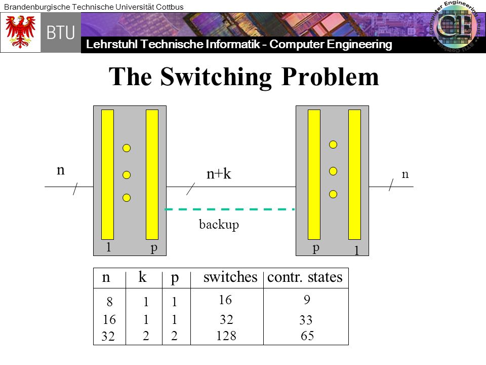
The Switching Problem n n+k n k p switches contr. states n backup 1 p
8 1 1 16 9 16 1 1 32 33 32 2 2 128 65
56
Faults and Repair Actions
1. Line- break: Section of a line is interrupted use spare wire! 2. Line- short to GND: Section of a line is connected to GND use spare wire! 3. Dynamic coupling between adjacent line: a. Re-allocate lines in bundle b. Insert grounded line for decoupling 4. Bridge between lines: a. Feed both lines with same signal b. Make one line „floating“

57
Single Line Replacement
Fault Signal s0 s1 s2 s3 s4 (k-1) Bachup b0 b1 b2 Overhead: 2k switches, (k+1) logic states for 1 backup line 2pk switches, p (k+1) logic states for p backup lines
 Bachup. b0. b1. b2. Overhead: 2k switches, (k+1) logic states for 1 backup line. 2pk switches, p (k+1) logic states for p backup lines.")
58
Inserting Lines for Decoupling
fault Signal s0 s1 s2 s3 s4 (k-1) Backup b0 b1 b2 Multiple line insertion for de-coupling requires multiple Shifts of lines, multiple switches and states!
 Backup. b0. b1. b2. Multiple line insertion for de-coupling requires multiple. Shifts of lines, multiple switches and states!")
59
Repair Mechanisms Buses with „extra“ backup lines that need specific configuration for repair generate high cost in terms of switches and administration due to many „logic states“ of the bus section. Such repair schemes are not suited to re-organize neighborhood relations on buses for de-coupling of lines. Try to cover all relevant fault conditions by a small set of states using permutation of lines!

60
Reconfiguration for De-Coupling
2-Way Switches may be used! i i k k i i k k … can help to minimize dynamic coupling faults!

61
Characteristics of 6 / 8 Wire Bundles
Given a bundle of 6 or 8 bus lines: Are there any permutations that create all-new neighbors for every single line in order to eliminate coupling faults? NNP6 NNP NNP82 NNP83 6 lines lines 0 - 2 0 - 2 0 - 3 0 - 5 1 - 6 1 - 5 1 - 7 1 - 4 2 - 0 2 - 7 2 - 4 2 - 0 3 - 5 3 - 0 3 - 6 3 - 5 4 - 7 4 - 6 4 - 2 4 - 1 5 - 3 5 - 1 5 - 0 6 - 1 6 - 4 6 - 3 5 - 3 7 - 4 7 - 2 7 - 1

62
6 Wires: Permutations and Replacement
Administration: Input wire 4 logic states for 2 sw.-columns mapping 1st switching column 2nd switching column 2 extra. wires 3rd switching column 6 logic states for Selected backup lines 3 sw.-columns Replacement possible by lines # (2 sw. col.) 1 extra. wire Line selected for backup
 1 extra. wire. Line selected. for backup.")
63
Selection of Permutations
All single faults must be repairable by selecting a minimum set of permutations. Those lines that can act as replacement for most of the others are selected for „backup lines“. By permutation, also non-faulty functional lines are re-arranged. No permutation used for repair must map a functional line to a faulty line.

64
Permutations for 8-Wire-Bundles
New-neighborhood Pair-wise symmetrical NNP1 NNP2 NNP3 PW1 PW2 PW3 0 - 2 0 - 3 0 - 5 0 - 1 0 - 6 0 - 4 1 - 6 1 - 5 1 - 7 1 - 0 1- 3 1 - 7 2 - 0 2 - 7 2 - 4 2 - 3 2 - 4 2 - 5 3 - 5 3 - 0 3 - 6 3 - 2 3 - 1 3 - 6 4 - 7 4 - 6 4 - 2 4 - 5 4 - 2 4 - 0 5 - 3 5 - 1 5 - 0 5 - 4 5 - 7 5 - 2 6 - 1 6 - 4 6 - 3 6 - 7 6 - 0 6 - 3 7 - 4 7 - 2 7 - 1 7 - 6 7 - 5 7 - 1

65
8 Wires: Permutations and Replacement
Selected backup Selected backup wires 2 lines selected for backup!

66
8 Wires: Permutations and Replacement
4 lines selected for backup!

67
Overhead / Coverage for 6-Line-Bundle
Spare. lines / Switches Faults 0/ / / 24 Single line fault - + + Dyn. coupl. faults + + + Double line faults - - 50%

68
Overhead / Coverage for 8-Line-Bundle
Spare Lines (out of 8) / Switches Faults 0/ / / 32 3 / 32 4/ 32 Single fine fault - + + + + Dyn. coupl. fault + + + + ++ ++ Double line faults - - 20% 30% 100 % Note: The number of switches is reduced by a factor of 2 if full 2-way-switches with 2 inputs / 2 outputs are used!
 / Switches. Faults. 0/ 16 1 /48 2 / / 32. 4/ 32. Single. fine fault Dyn. coupl. fault Double. line faults % 30% 100 % Note: The number of switches is reduced by a factor. of 2 if full 2-way-switches with 2 inputs / 2 outputs are used!")
69
Results Bus segments can favorably be organized into bundles
of 8 lines for reconfiguration. Wider bundles require even more columns of switches. In a bundle of 8 lines, all single faults can be repaired either by one backup line and 3 columns of switches or two backup lines and 2 columns with 6 / 4 logic states. Two columns with 4 states also allow for two alternative modes of changing neighborhood relations for de-coupling. It also covers a fraction of double-line faults. A full coverage of double-line-faults requires 4 backup lines and 2 columns of switches or 2 backup lines and 4 columns.

70
Administration Scheme
lines in / Switches Switches out 0‘ out 1 1‘ 1 2 2‘ 2 3 3‘ 3 4 A B 4‘ B A 4 5 5‘ 5 6 6‘ 6 7 7‘ 7 Decode Config - bits Decode C1 C2 C2 C1 Matching Config - Config - Logic Logic

71
Processor-Based Bus Test
Master Bus reflector data lines Bus Bus Master Master reflector select Test Processor invert control clock

72
Test and Fault Diagnosis
S C BM S C S C BM S C BM S C S C BM BM S C S C S C S C BM Test Processor Segment Status List

73
Test Procedure & Fault Management
Upcoming: Test Procedure & Fault Management Test-Processor can „reset“ control of bus sections. Test processor runs diagnostic test to identify faulty lines. In case of faults, „trial and error“ test to identify faulty line segment(s). Test Processor keeps „fault list“ for redundancy management & supervision.
. Test Processor keeps „fault list for redundancy. management & supervision.")
74
Summary A simple scheme of re-arranging bus sections for repair of
permanent faults. Simple control scheme based on few logic states. Modular approach based on bundles of lines is scalable to cover wider buses. Should work well with NoCs. Compatibility with regular schemes for bus test based on a dedicated test processor device. The number and the electrical effect of switches in complex bus systems may still cause problems.

75
5. Diagnostic Tests Fault diagnosis by diagnostic (self-) test is possibly the real bottleneck in logic BISR!
 test is possibly the real bottleneck in logic BISR.")
76
Fault Diagnosis Memory cells are either to diagnose in case of faults
affecting single cells. BIST is possible. Diagnostic tests of buses that have to discover a single faulty line are straightforward. They can easily find which wires are affected, but not where the fault is. Detecting a fault gate or even transistor in a logic block is a much more challenging problem. Diagnosis must be compatible with methods of test response compaction used in scan testing. Intelligent encoding for test responses! ... such as done by U. Potsdam and Infineon!

77
Combinational Logic Fault Diagnosis
Input - FFs Output FFs Faults can occur within specific gates, on interconnects, or in a „distributed“ manner. Identifying a specific fault gate or line is not easy at best and sometimes close-to impossible by logic testing.

78
Logic Test Comb. Logic (pseudo-) (pseudo-) inputs outputs Output Input
vector Input vector

79
Scan Path Technology Comb. Logic Scan-in Scan-out (pseudo-) inputs
outputs ff Comb. Logic ff ff ff ff ff ff ff ff ff ff Scan-in Scan-out Output vector Input vector

80
Test response compactor
Scan-based Logic Test Compacted / encoded test information De-compactor C L C L Coding Test response compactor Diagnosis

81
Fault Diagnosis on Compacted Output Data
Scan input Generator (De - Compactor ) scan clock d - value d d d d d d d 1 2 3 4 5 6 storage & & & & & & & MISR Ref. MISR MISR clock : k * scan - clock compare * patented , U. Potsdam and Infineon Technologies AG
 scan clock. d. - value. d. d. d. d. d. d. d storage. & & & & & & & MISR. Ref. MISR. MISR. clock. : k * scan. - clock. compare. * patented. , U. Potsdam and. Infineon Technologies. AG.")
82
6. A Lot of Work to Do Logic fault diagnosis
Efficient logic self repair Redundancy supervision and management Resource management under fault conditions Repair functions for interconnects Overall system-level fault management

Ähnliche Präsentationen


