Präsentation herunterladen
Die Präsentation wird geladen. Bitte warten

1
Mesoporous silica low-k dielectric films:
Deposition, characterisation and integration Chris Murray Chemnitz University of Technology, Center of Microtechnologies, Germany

2
Contents Where is Chemnitz? Why low-k?
Sol-gel route to mesoporous silica Characterisation techniques Integration Conclusions

3
Where’s Chemnitz?

4
Why low k? The RC delay problem
Upper Metal Layer R=2rL/PT C=2(CLL+CV) = 2ke0(2LT/P+LP/2T) RC=2rke0(4L2/P2+L2/T2) W S CLL T Interconnect P CV=CLG The time delay in the interconnection of ICs is a performance limiting factor when feture size is scaled down below 0.25um. This is a typical example of a multilevel interconnect system where P=W+S ans W=S. The metal thickness T and the dielectric thickness above and below are equal. CLLis the lateral line-to-line capacitance, CV is the vertical layer to layer capacitance andCLG is the line to ground capacitance. The RC time delac is dependent on two material factors: the resistivity of the interconnecting metal, and the dielectric constant of the insulator. This simple first order model was used by Bohr to estimate the interconnect RC delay When the interconnect spacing is less than 0.3um, the interlayer capacitance(CV or CLG) is very small compared withthe total capacitance. The total capacitance is dominated by line to line capacitance. Almost 90% of the total capcaitance comes from the line to line capacitance at sub-0.25um feature sizes. Therefore reducing Line to line capacitance is one of the most critical issues for sub-0.25um IC devices. Another advantage of lower total capacitance is that crosstalk and power dissipation are reduced. Lower Metal Layer M. Bohr, Tech. Digest IEEE Int. Electron. Devices Meeting 1995 p. 241
 = 2ke0(2LT/P+LP/2T) RC=2rke0(4L2/P2+L2/T2) W. S. CLL. T. Interconnect. P. CV=CLG. The time delay in the interconnection of ICs is a performance limiting factor when feture size is scaled down below 0.25um. This is a typical example of a multilevel interconnect system where P=W+S ans W=S. The metal thickness T and the dielectric thickness above and below are equal. CLLis the lateral line-to-line capacitance, CV is the vertical layer to layer capacitance andCLG is the line to ground capacitance. The RC time delac is dependent on two material factors: the resistivity of the interconnecting metal, and the dielectric constant of the insulator. This simple first order model was used by Bohr to estimate the interconnect RC delay. When the interconnect spacing is less than 0.3um, the interlayer capacitance(CV or CLG) is very small compared withthe total capacitance. The total capacitance is dominated by line to line capacitance. Almost 90% of the total capcaitance comes from the line to line capacitance at sub-0.25um feature sizes. Therefore reducing Line to line capacitance is one of the most critical issues for sub-0.25um IC devices. Another advantage of lower total capacitance is that crosstalk and power dissipation are reduced. Lower Metal Layer. M. Bohr, Tech. Digest IEEE Int. Electron. Devices Meeting 1995 p")
5
Why Low k? As the dimensions of ULSI devices scale to smaller features, the resistance-capacitance (RC) delay of the metal interconect becomes performance limiting. The gate delay is important only for device features larger than 1um. When the feature size shrinks to less than 0.5um, the interconnect RC delay becomes dominant. You can see the quadratic nature of the RC delay...lets take a closer look at how it originates.
 delay of the metal interconect becomes performance limiting. The gate delay is important only for device features larger than 1um. When the feature size shrinks to less than 0.5um, the interconnect RC delay becomes dominant. You can see the quadratic nature of the RC delay...lets take a closer look at how it originates.")
6
Metals Exchanging Cu for Al reduces delay by about 35% although many problems exist for integration.

7
Roadmap (1999 ITRS, International SEMATECH)
Interconnect Technology Requirements - Near Term

8
A range of dielectrics are becoming commercially available
At the April 98 MRS meeting on Low k materials there were 5 papers on ultra low k materials (k<2.3) - four were on porus silica and one was on porous MSQ. There were 23 papers at the 1999 MRS Low Dielectric Constant Symposium, ranging from porous SiO2(7), MSQ (2), parylene (2), SiON(1), HSQ(1), a-CF(6), airgaps (2) & porous polymers (2) HSQ = Hydrogen silsesquioxanes e.g. Dow Corning‘s Fox = Flowable Oxideused in TI‘s0.5um process and Philips latest BiCMOS process QuBiC3 MSQ = Methyl silsesquioxanes HOSP is a siloxane polymer inorganic / organic hybrid for spin on from ALLIED SIGNAL CVD low k such as APPLIED MATERIALS BLACK DIAMOND FLARE AND Nanoglass are also from ALLIED SIGNAL Morey & Asthana, Solid State Technology, Vol. 2, No. 6, June 1999 p.71,
 - four were on porus silica and one was on porous MSQ. There were 23 papers at the 1999 MRS Low Dielectric Constant Symposium, ranging from porous SiO2(7), MSQ (2), parylene (2), SiON(1), HSQ(1), a-CF(6), airgaps (2) & porous polymers (2) HSQ = Hydrogen silsesquioxanes e.g. Dow Corning‘s Fox = Flowable Oxideused in TI‘s0.5um process and Philips latest BiCMOS process QuBiC3. MSQ = Methyl silsesquioxanes. HOSP is a siloxane polymer inorganic / organic hybrid for spin on from ALLIED SIGNAL. CVD low k such as APPLIED MATERIALS BLACK DIAMOND. FLARE AND Nanoglass are also from ALLIED SIGNAL. Morey & Asthana, Solid State Technology, Vol. 2, No. 6, June 1999 p.71,")
9
Introduction of pores to lower k
By making SiO2 porous, the effective k value is reduced An overview of our work on porous silica: Why porous silica? How xerogel films are made chemistry Properties of the films in comparison to commercially available mazerial Integration Issues Outlook As the RC interconnect delay time becomes dominant at featauresizes in the submicron range, the switch to lower resistivity copper conductors and low k intermatal dielectrics is already underway. This diagram shows how the dielectric constant of SiO2 is expected to decrease with the increasing porosity. At 0% porosity, bulk k = 4, at 100% porosity k= 1 (air) Comprimise in the middle between low k and mechanical stability
 Comprimise in the middle between low k and mechanical stability.")
10
Sol Gel Processing Sol Gel Science, Brinker & Scherrer, Academic Press, 1990, p. 1

11
General Sol-Gel Process Flow for Porous SiO2
How do we make a porous film? Start with spinning on a SOL, a liquid containing solvents and chains of SiO2. These grow and link and form a solid network of SiO2 with solvent containing pores. This is called a gel. The film must then be dried by removing the solvents without collapsing the pore structure. Therein lies the problem!

12
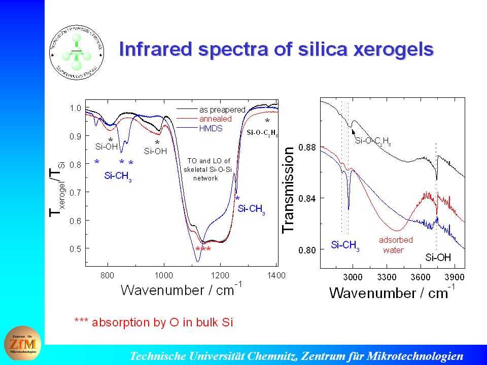
Mesoporous xerogel low-k film production
Spin on Post-spin on gelation Drying / Annealing 450°C Hydrophobisation with HMDS Pre-spin on gelation Precursor & catalyst mixing Precursor = TEOS, water, solvent, catalyst hydrolysis / condensation reactions n-type 150 mm Si wafers Si-O-Si porous network forms after spin-on Replace hydrophylic surface -Si-OH groups with hydrophobic -Si-O-Si(CH3)3 Porosity controlled by changing the time allowed for gelation reactions before and after spin on We made 5 samples with range of porosities Round robin to each characterisation method, which I will now describe 5 process variations = range of dielectric constants
3. Porosity controlled by changing the time allowed for gelation reactions before and after spin on. We made 5 samples with range of porosities. Round robin to each characterisation method, which I will now describe. 5 process variations = range of dielectric constants.")
13
Film properties Nanoglass is a trademark of Allied Signal / Honeywell
This table shows the properties of the Nanoglass and TUC materials. They are quite similar even though the TUC material does not require a solvent exchange step. Note the higher modulus of elasticity of the TUC material N/a = not available (no data found) Nanoglass is a trademark of Allied Signal / Honeywell
 Nanoglass is a trademark of Allied Signal / Honeywell.")
14
Film Characterisation
TEM of Pt imprint of xerogel film Atomic Force Microscopy very smooth film surface maximum height Rmax < 8 nm mean roughness Ra < 1 nm

16
Ellipsometric Porosimetry (EP)
pump PC P adsorptive laser sample detector Ellipsometric Porosimetry (EP) n porosity AND , toluene absorption pore size and distribution, pore interconnectedness OP=55% FP=54% CSA=260 m2 cm-3 Multi-angle single frequency (=632.8 nm) EP measures the film refractive index to calculate the ‘full’porosity using the Lorentz-Lorenz equation. TOP DIAGRAM It also measures the change in ellipsometric characteristics and during desorption of toluene vapor and calculates the ‘open’ porosity, i.e. that portion of the pore network available to toluene penetration. BOTTOM DIAGRAM LEFT If the full and open porosities are equal, all the pores in the film are said to be interconnected. Here is such a film BOTTOM DIAGRAM LEFT The pore size distribution (PSD) is also calculated from ellipsometric optical constant changes during toluene desorption using the Kelvin and BET equations. The cumulative surface area is calculated by integrating the PSD data for a cylindrical pore model. BOTTOM DIAGRAM RIGHT The accuracy is estimated to be 3 %.
 n porosity. AND. , toluene absorption. pore size and distribution, pore interconnectedness. OP=55% FP=54% CSA=260 m2 cm-3. Multi-angle single frequency (=632.8 nm) EP measures the film refractive index to calculate the ‘full’porosity using the Lorentz-Lorenz equation. TOP DIAGRAM. It also measures the change in ellipsometric characteristics and during desorption of toluene vapor and calculates the ‘open’ porosity, i.e. that portion of the pore network available to toluene penetration. BOTTOM DIAGRAM LEFT. If the full and open porosities are equal, all the pores in the film are said to be interconnected. Here is such a film BOTTOM DIAGRAM LEFT. The pore size distribution (PSD) is also calculated from ellipsometric optical constant changes during toluene desorption using the Kelvin and BET equations. The cumulative surface area is calculated by integrating the PSD data for a cylindrical pore model. BOTTOM DIAGRAM RIGHT. The accuracy is estimated to be 3 %.")
17
Laser Induced Surface Acoustic Waves (LSAW)
Laser Pulse SAW Piezoelectric pickup Velocity (m s-1) Frequency (MHz) V film thickness, density, elastic modulus and Poisson‘s ratio new surface acoustic wave technique, LSAW, measures the velocity dispersion of laser-generated wideband surface acoustic waves as a function of frequency as they travel through the film and substrate . DIAGRAM dispersion depends on the properties of the layer (thickness, elastic modulus, Poisson’s ratio and average film density). The large mismatch between the acoustic properties of the Si wafer substrate and the porous silica film makes this method well suited to this task. TEXT & DIAGRAM Using the measured film thickness and assuming a constant Poisson’s Ratio (v = 0.21 in all cases), absolute values of average film density and elastic modulus can be determined by curve fitting.
 Frequency (MHz) V film thickness, density, elastic modulus and Poisson‘s ratio. new surface acoustic wave technique, LSAW, measures the velocity dispersion of laser-generated wideband surface acoustic waves as a function of frequency as they travel through the film and substrate . DIAGRAM. dispersion depends on the properties of the layer (thickness, elastic modulus, Poisson’s ratio and average film density). The large mismatch between the acoustic properties of the Si wafer substrate and the porous silica film makes this method well suited to this task. TEXT & DIAGRAM. Using the measured film thickness and assuming a constant Poisson’s Ratio (v = 0.21 in all cases), absolute values of average film density and elastic modulus can be determined by curve fitting.")
18
Nanoindentation Can measure Can’t measure !! Careful
elastic modulus hardness Can’t measure porosity !! Careful sample and substrate effects for films < 1µm A known force is applied to a geometrically-shaped indenter which is driven into the film sample to a measurable depth .DIAGRAM Using analytic or finite element modelling, some of the material mechanical properties can be derived from the indentation load-displacement data. LOAD CURVE Porosity information is not available using nanoindentation. The accuracy depends on film thickness, film structure and the mismatch between film and substrate elastic constants. Despite the relative complexity involved in interpreting the results, this method is becoming widely used in the industry. UNKNOWN - the reaction of porous materials!!!!!!!!!!!!!!!

19
Porosity Results LSAW & RBS agree to within experimental error
EP up to 20% lower than RBS How realistic is the reference density? Film thickness, dielectric constant values and porosity values are shown here for each of the 5 process variations, labelled A to E k clearly decreases with increasing porosity as expected. Good correlation between measurement techniques Full & open porosity match - pores all interconnected However the porosity values themselves vary between the three techniques. LSAW values are about about 5% higher than RBS, and EP about 12-20% less than RBS. The LSAW porosities calculated using a skeletal density value of tridymite, i.e g cm-3, This value was confirmed by RBS data on a 490nm thermal SiO2 bulk film - however the fractal nature of these films, and the inclusion of F and C in the skeleton due to processing may mean that the value is too small, which would bring the LSAW and RBS porosity down. But is EP really correct?? * Film reference density used for LSAW and RBS porosity = 2.26 g cm-3 RBS measured thermally grown dense SiO2 = 2.24 0.1 g cm-3

20
Combine LSAW or RBS mean film density with EP open porosity
Skeletal Density Combine LSAW or RBS mean film density with EP open porosity skeletal density skeleton = g cm-3

21
Surface Area & Pore size r(mean) increases and pore surface area decreases as porosity increases i.e. fewer, larger pores Elastic Modulus & Hardness Modulus and hardness correlate well with porosity and each other Overestimation of nanoindentation modulus by >20% due to substrate effects Refinements needed TOP: shows surface area in m3 cm-3 and mean pore radius Pore radius increases as porosity increases, but the cumulative surface are decreases. So, larger pores but fewer of them. This is typical for such films BOTTOM: Elastic modulus and hardness results low - former results were higher - process dependent. Nanoindentation modulus higher than LSAW - possible due to uncertancies regarding film crushing or pile-up. This is a recognised problem for soft films on hard substrates. More work to be done on to refine accuracy

22
Patterning of xerogel thin films using PECVD SiO2 cap layer
Cu TiN SiO2 Xerogel Trench etch: ICP using CF4 / CHF3 trench depth: 500 nm cap: 50 nm PECVD SiO profile angles > 85° no undercut of cap layer bowing was observed at large open areas Trench after MOCVD TiN deposition Si xerogel Etched 0.2 µm trenches cap xerogel Si MOCVD TiN

23
Davies & Corbett Solid State Tech.,
Outlook Porous silica materials posess lowest k values Many integration issues remain to be resolved Davies & Corbett Solid State Tech., Vol. 43, Issue 4, April, 2000

24
How do we define porosity?
skeleton pore

25
Ellipsometric Porosimetry
Can measure film thickness refractive index “full” and “open” porosity pore size distribution pore connectivity cumulative surface area Can’t measure elastic modulus !! Careful “full” porosity calculated using reference refractive index value of dense SiO2 toluene cannot penetrate pores of radius < 0.3 nm APPARATUS PHOTO Can obtain lots of information Mechanical characteristics such as elastic modulus are not available using EP. This method is also non-destructive, fast and can be applied to multilayers with known optical characteristics. Non-destructive Simple vacuum equipment Non-hazardous adsorptive

26
Laser Induced Surface Acoustic Waves
Can measure average film density elastic modulus Can‘t measure Pore size distribution surface area !! Careful Need a film skeletal density value for porosity calculations e.g. dense SiO2 Porosity can then be calculated using a value of film skeletal density – the simplest case being that of bulk SiO2. The inherent accuracy of the technique is related to film thickness and average density – for these samples of the order of 3 % for porosity and 0.5 GPa for elastic modulus. results are not point-specific. the only method which allows porosity information and mechanical properties to be gained at the same time. special patterned oscillating sensor substrates are not required - better adapted to serve in volume production. non-destructive, requiring relatively simple setups and results can be achieved in minutes. application of the method to multilayer systems is more complex Non-destructive / non-invasive No patterned substrates or vacuum chamber required Only technique which provides density/porosity and mechanical characteristics

27
Measurement Capabilities
Comparing POROSITY = RBS, LASW, EP Elastic Modulus = LSAW, Nanoindentation Proven Possible Proven for dense films

28
Conclusions Can´t use skeleton = SiO2
Porosity depends on choice of reference values used in calculations Can´t use skeleton = SiO2 ? Can we still use nskeleton = nSiO2 EP shows pores are interconnected LSAW mean film density correlates with RBS LSAW or RBS mean film density combined with EP open porosity gives film skeletal density skeleton = g cm-3 Elastic modulus values low, hard to measure with accuracy Techniques should refine themselves as the sample database grows

Ähnliche Präsentationen